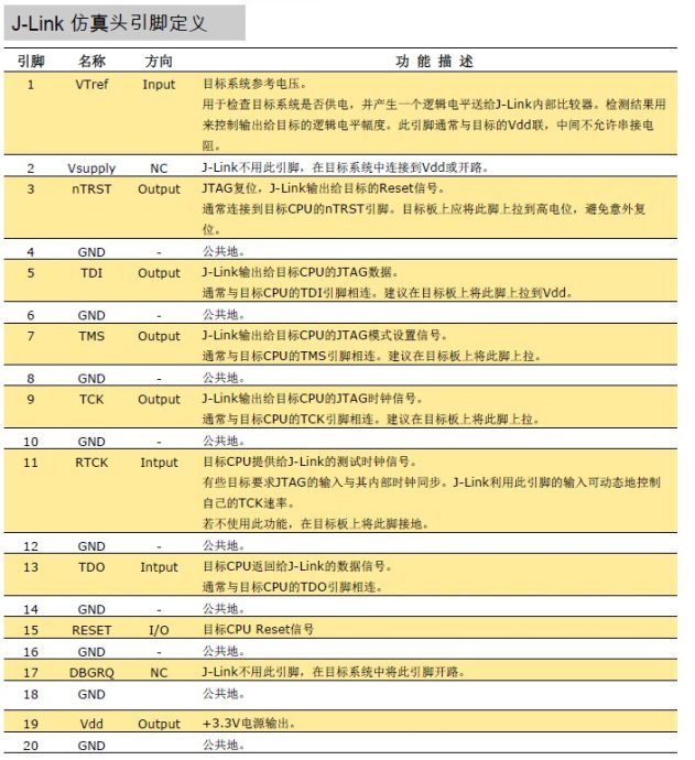
|
DBGACK
|
-
|
This pin is connected in the RVI run control unit, but is not supported in the current release of the software. It is reserved for compatibility with other equipment to be used as a debug acknowledge signal from the target system. It is recommended that this signal is pulled LOW on the target.
|
|
DBGRQ
|
-
|
This pin is connected in the RVI run control unit, but is not supported in the current release of the software. It is reserved for compatibility with other equipment to be used as a debug request signal to the target system. The RVI software maintains this signal as LOW.
When applicable,RVI uses the scan chain 2 of the processor to put the processor in debug state. It is recommended that this signal is pulled LOW on the target.
|
|
GND
|
-
|
Ground.
|
|
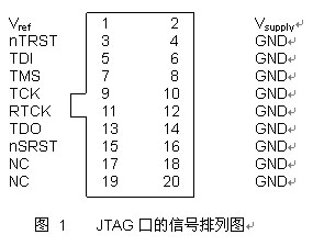
nSRST
|
Input/output
|
Active Low output from RVI to the target system reset, with a 4.7kΩ pull-up resistor for de-asserted state. This is also an input to RVI so that a reset initiated on the target can be reported to the debugger.
This pin must be pulled HIGH on the target to avoid unintentional resets when there is no connection.
|
|
nTRST
|
Output
|
Active Low output from RVI to the Reset signal on the target JTAG port, driven to the VTref voltage for de-asserted state. This pin must be pulled HIGH on the target to avoid unintentional resets when there is no connection.
|
|
RTCK
|
Input
|
Return Test Clock signal from the target JTAG port to RVI. Some targets must synchronize the JTAG inputs to internal clocks. To assist in meeting this requirement, you can use a returned, and retimed, TCK to dynamically control the TCK rate. RVI provides Adaptive Clock Timing, that waits for TCK changes to be echoed correctly before making more changes. Targets that do not have to process TCK can ground this pin.
RTCK is not supported in Serial Wire Debug (SWD) mode.
|
|
TCK
|
Output
|
Test Clock signal from RVI to the target JTAG port. It is recommended that this pin is pulled LOW on the target.
|
|
TDI
|
Output
|
Test Data In signal from RVI to the target JTAG port. It is recommended that this pin is pulled HIGH on the target.
|
|
TDO
|
Input
|
Test Data Out from the target JTAG port to RVI. It is recommended that this pin is pulled HIGH on the target.
|
|
TMS
|
Output
|
Test Mode signal from RVI to the target JTAG port. This pin must be pulled HIGH on the target so that the effect of any spurious TCKs when there is no connection is benign.
|
|
Vsupply
|
Input
|
This pin is not connected in the RVI unit. It is reserved for compatibility with other equipment to be used as a power feed from the target system.
|
|
VTref
|
Input
|
This is the target reference voltage. It indicates that the target has power, and It must be at least 0.628V. VTref is normally fed from Vdd on the target hardware and might have a series resistor (though this is not recommended). There is a 10kΩ pull-down resistor on VTref in RVI.
|